Features
- Low noise despite incorporating with first-stage FET protection circuit
- Low offset voltage is maintained over a wide temperature range (0 to 50 degrees C = 32 to 122 degrees F)
- Equipped with over-voltage protection, over-current protection, and high-temperature protection for safe use
Measurement demonstration
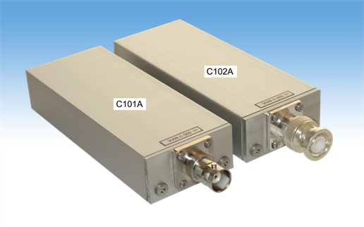
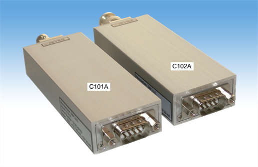
C101A and C102A Specifications
(1) Charge-sensitive amplifier circuitry section
| Item | Specification | Remarks |
| Decay time constant | 0.7 ms (1GΩ // 0.7 pF) | – |
| Connector with detector | BNC-J (C101A) BNC-P (C102A) | – |
| Input coupling | AC | – |
(2) Differential circuitry section
| Item | Specification | Remarks |
| Time constant | 48 μs | – |
| Pole zero cancel (PZC) | Yes, changeable | User replacement is not supported. |
(3) Output buffer section
| Item | Specification | Remarks |
| DC offset voltage | Within ± 5 mV | 0 ℃ – 50 ℃ |
| Output impedance | 51 Ω | – |
(4) Noise
| Item | Specification | Remarks |
| 0 pF Load | Less than 1.3 keV | 25℃, Si detector equivalent at 88 keV, shaping time constant at 2 μs |
| 100 pF Load | Less than 2.5 keV | Same as above |
(5) Response characteristics
| Item | Specification | Remarks |
| Output polarity to input | Invert | – |
| Charge sensitivity | Approx. -11 mV / fC | – |
| Rise time | Less than 50 ns | 10 % to 90 %, 100 pF Load |
(6) Bias voltage input for detector
| Item | Specification | Remarks |
| Bias resister | 1 GΩ | – |
| Applicable voltage | Within ± 500 V | – |
| Built-in LPF time constant | 10 ms (1 MΩ、0.01 μF) | – |
(7) Test pulse input
| Item | Specification | Remarks |
| Coupling capacitor | 0.5 pF | – |
| Input impedance | 51 Ω | – |
(8) Protections
| Item | Specification | Remarks |
| First-stage FET protection | Over voltage protection circuit | – |
| Over current protection for ±12V power input | PTC Resettable Fuse | Itrip: 300mA |
| Over temperature protection | The amplifier turns off when the internal temperature reaches 65 ℃, and automatically returns to normal when the temperature drops. | – |
(9) Connector for external (signal, power supply, etc.)
| Item | Specification | Remarks |
| Type | D-Sub 9 pins, male | – |
| Pins assignment | Pin#1: GND Pin#2: GND Pin#3: Signal OUT Pin#4: +12V IN Pin#5: Detector bias voltage IN (Max. ± 500 V) Pin#6: RXD for offset control Pin#7: TXD for offset control Pin#8: Test pulse IN Pin#9: -12V IN | – |
(10) Power supply
| Item | Specification | Remarks |
| Ratings | DC +12V 40 mA, DC -12V 25 mA | Voltage range: Within ±5% |
(11) Operating environment condition
| Item | Specifications | Remarks |
| Ambient temperature and humidity | 0 ℃ – 50 ℃, Less than 80 %RH | – |
| Where to use | Indoor | – |
(12) Dimensions and weight
| Item | Specifications | Remarks |
| Dimensions | 40 mm x 20 mm x 101 mm (Excluding connectors) | – |
| Weight | Approx. 107 g (C101A), Approx. 115 g (C102A) | Typical |